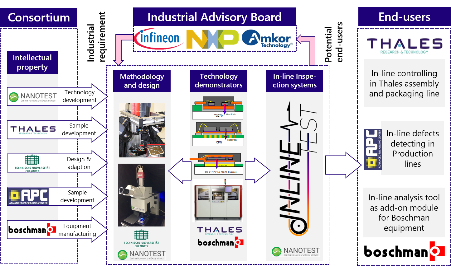
The Project
is a European funded project that targets the design, realization, deployment and test of two novel in-line inspection systems for micro/nano-electronic components.
For the first time, the fast, contactless and non-destructive full-field thermometric methods of Pulse-Infrared Thermography (PIRT) and Thermoreflectance (TR) are exploited to enable 100% in-line production monitoring. This will be done by adapting and upgrading existing lab prototypes for both methods to the challenges of real-life in-line testing, enhanced by hard- and software innovations. For validation under real-life conditions, both failure analytical method’s hard- and software will be customized and integrated into two production lines and demonstrated on two encapsulated power multi-chip module (MCM) components and one in-line production tool at the project partners. Three global players in micro/nano-electronics in Europe accompany this endeavor on the board of industrial advisors.
Thermography-Based Quality Assessment
Contactless, non-destructive in-line testing has been the ultimate goal for quality assessors and process managers for decades. Thermography holds the key to finally open that door and to revolutionize production line quality control. Hidden flaws like voids, cracks, delaminations and tilts burried under mold compound are potential factors for early failures and decreased quality output and are not detectable just by visual inspection.
Thermography can be used to analyze a component of sub-component with a surface of nearly any kind. Classical infrared thermography allows observation of non-reflecting surfaces while the newer thermoreflectance thermography is capable of monitoring reflecting surfaces such as bare dies, glass or even polished metal. Both techniques, though based on slightly different phenomena, offer the same gain of information about the thermal stack below the surface under observation.
new_releases RESULTS
INFAS
Inline Failure Analysis System
INFAS is the centerpiece of and a modular and a highly is a modular and highly customizable failure analysis system for installation in production lines for in-line failure analysis and quality assessment. It allows detection of a wide range of defects in various types of modules and components by means of contactless and non-destructive techniques.
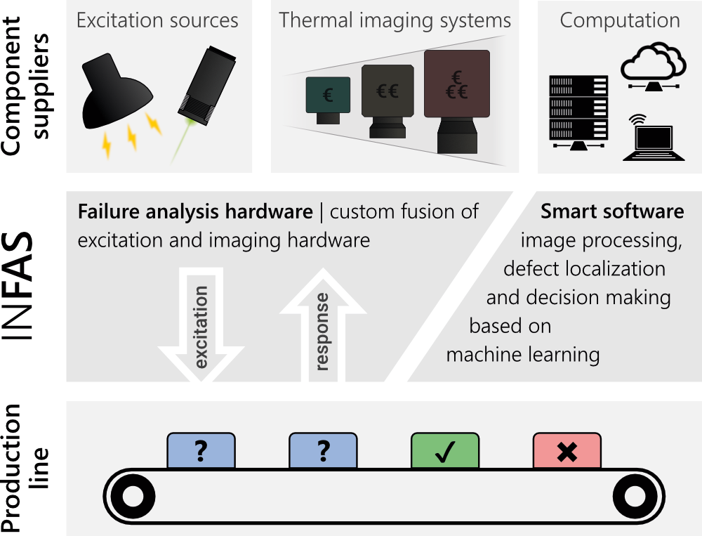
The shown schematic depicts the modular principle of INFAS.
Any excitation source that fits the devices under test may be used, including laser diodes, Eddy current or flash lamps.
Image acquisition by infrared thermography may draw on a variety of infrared cameras, ranging from cost-effective to very high-end systems. Depending on the required resolution, also the optics for the cameras are free of choice and no limit is set by INFAS.
The decicive factor for quality assessment is decision-making. A powerfull, yet compact and efficient software handles image acquisition and analysis. An important part of the analysis is TSR - thermal signal reconstruction - greatly improving the contrast of images to boost chances of flaw detection and reduces the minimum detectable necessary flaw magnitude.
Machine learning allows the software to judge the devices under test based on the acquired thermal images for fully automized 100% inline quality control.
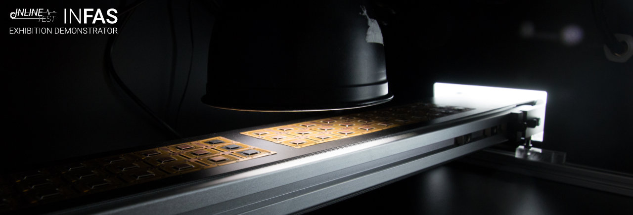
The INFAS exhibition demonstrator incorporates a conveyor belt through a box with a flash lamp and a low budget infrared camera. With the integrated PC running the acquisition and analysis software, this first functional project demonstrator is capable of detecting voids in sinter layers, molding compound and carbon fiber reinfoced polymers (CFRP).
Download the flyer to learn more: infas_flyer_2019_web.pdf (430 KB)
TIFAS IR
Thermal Imaging-based Failure Analysis System based on infrared thermography
TIFAS IR could initiate a paradigm shift in failure analyis. Never-seen simplicity, purity and focus on the thermal domain of failure analysis.
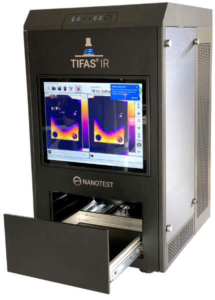
As an outcome of the INFAS development, learnings about hardware and system integration and software-based improvement of analysis techniques, a ready-to-use benchtop solution has been developed - TIFAS IR.
TIFAS IR is the world's first failure analysis system to be all-in-one regarding required components in hard- and software. It brings everything necessary to perform failure analysis on electrical components, mechanical parts, joints or other small objects potentially containing hidden defects. The range of detectable defects includes (amongst many others):
- Voids
- Cracks
- Delamination
- Inclusions
TIFAS IR brings laboratory and academic failure analysis down to desktop-scale and makes it quick to learn, easy to handle and cost-efficient to acquire. This is a novelty to the failure analysis market and will change the perception of infrared thermography in the industry.
With the aid of thermographic methods such as pulse and pulse-phase as well as lock-in thermography, paired with intelligent image processing, within seconds and partly automated a decision on a sample's integrity can be made. The use of a flash lamp as excitation source plays an important role to conduct pulse thermography quickly and reliably.
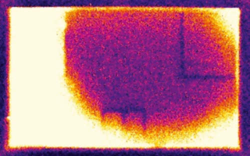
This IR image shows a large-area delamination in the sinterd silver layer under a DCB substrate. Already a delamination of less than 1 mm diameter is clearly visible.
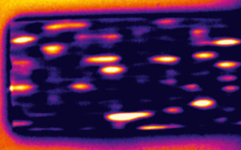
The entrapped air in a carbon fiber reinforced polymer caused by insufficient evacuation are clearly visible. The voids sizes range between 0.5 and 2 mm.
The investigation of multiple components at once can massively accelerate quality assessment. Visible defect sizes start at 500 µm, depending on their vertical position.
Download the flyer to learn more: tifas_flyer_2020_01.pdf (1010 KB)
Demonstration video
TIFAS TR
Thermal Imaging-based Failure Analysis System based on thermo-reflectance thermography
Infrared thermography-based failure analysis often requires surfaces to be highly emissive which often is achieved by coating surfaces with black paint. This is not an option in production lines as the black paint needs to be washed off afterwards. Thermo-reflectance allows avoiding surface treatment in the process as it builds on the physical properties of reflective surfaces and furthermore greatly enhances spatial resolution of acquired thermographic images.
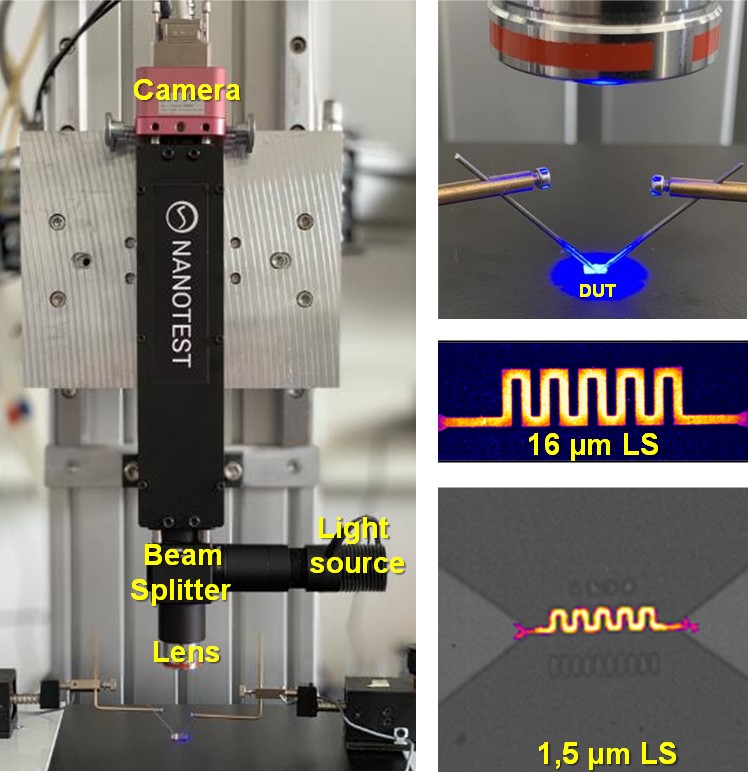
TIFAS TR is a compact and lightweight custom thermo-reflectance module. It allows temperature mapping on reflective surfaces with high lateral resolutions (down to 250 nm).The System consists of a camera with sensitive CMOS detector that comes with high full well capacity (200 ke-), a low read-out noise (3 e-), and high quantum efficiency of >78%.
Thermo-reflectance requires a light source as optical excitation source which is a selection of different LEDs that cover a wide range of wavelengths from 460 nm to 780 nm and also a broadband white light for multipectral illumination. This set of light sources allows measurments on all typical surfaces found in electronics, such as gold, aluminum, titanium, nicker, copper and chromium.
Besides avoiding the necessity of surface blackening, thermo-reflectance thermography comes with a list of advantages over infrared thermography:
- Measurement of reflective surfaces
- Higher spatial resolution (down to 250 nm)
- Low-cost and highly compact hardware
- Selective imaging by excitation wavelength
The pictures show typical measurement results on gold structures with 16 and 1.5 µm line width. Using the optimal wavelength for gold (530 nm) ensures high contrast of the thermal image.
Failure analysis on GaN HEMT by thermo-reflectance
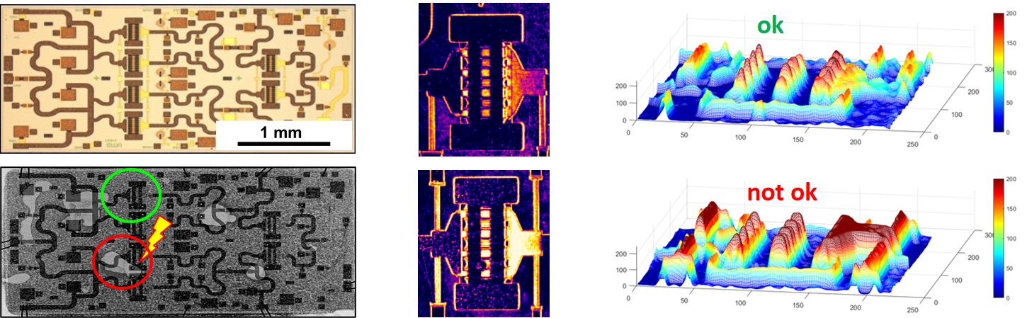
Thermo-reflectance imaging was used to locate hot spots in an HPA module. These hot spots can be caused by voids or cracks in the attach.
The right hand graphs show the results of the TR measurement on the HPA module. Two adjacent transistors show clearly different operating temperatures while operating with the same power dissipation. The cause of the temperature difference is a void in the attach beneath one of the transistors, which is clearly shown by an X-Ray analysis (bottom left image).
Height and Tilt Measurement
Optomechanical measurement system for determination of height variation and tilt
Tilt is an indicator for bad quality of die attach, chip or component placement, errorneous molding and many other flaws that may occur during processing and assembly. Fast and reliable tilt detection by contactless sensing technology is key to access of this quality assessment tool to the line.
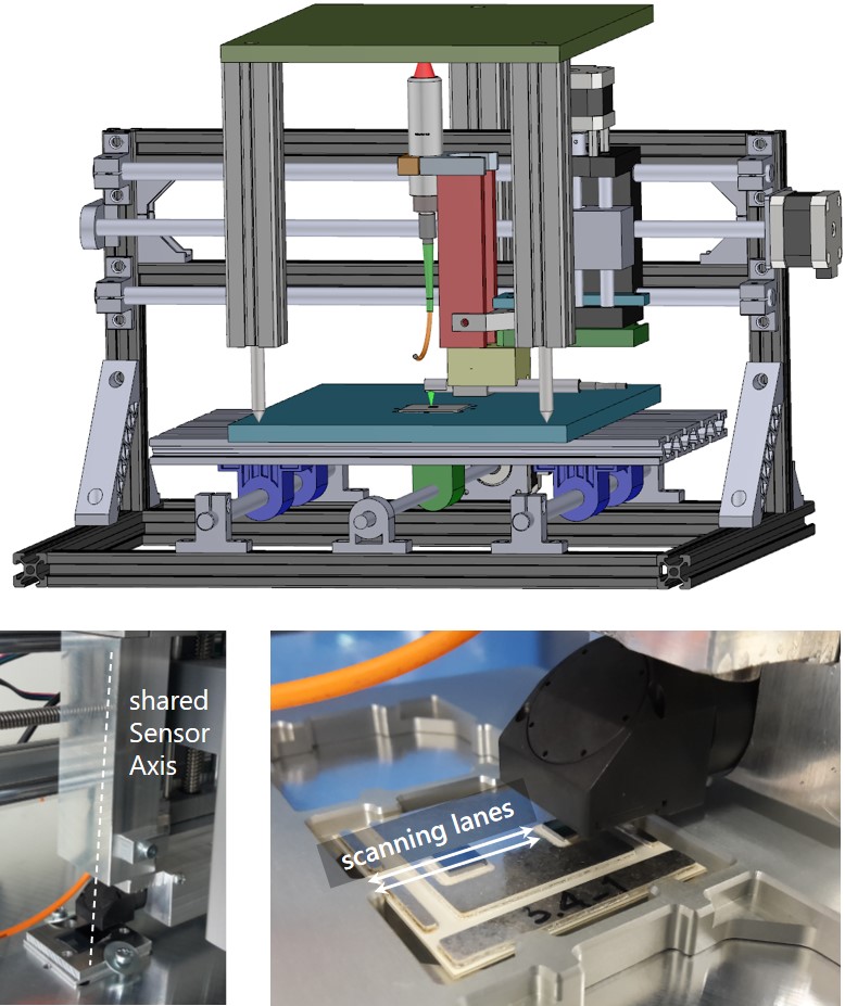
An inline-capable test bench was built, using 2 optical confocal white light sensors with a maximal resolution of up to 60 nm. The dual-scanner concept (scanning the sample and a reference plane simultaneously) allows the filtering of the mechanical noise affecting both sensors. The remaining noise (higher oscillation modes) and therefor the overall accurately measured depth of a line scan at perfect surfaces is below 1µm, on authentic samples up to 2 µm.
A Program was written, which identifies the chip surface, the flanks and levels the chip and substrate ground levels. Out of that, the height at the flanks can be calculated.
The table below lists some of the major characteristics of the measurement system regarding resolution and accuracy.
| System | Parameter | Typical | Maximal | Unit |
|---|---|---|---|---|
| Confocal sensor | Sampling rate | 1000 | 70 000 | Hz |
| Spot size | 50 | µm | ||
| Z resolution | ≪ 2 | 0.06 | µm | |
| Scanning unit | XY travel | 100 | 300 | mm |
| Speed | 2 | 10 | mm/s | |
| XY resolution | 50 | 20 | µm |
Measurement results - line scan of package
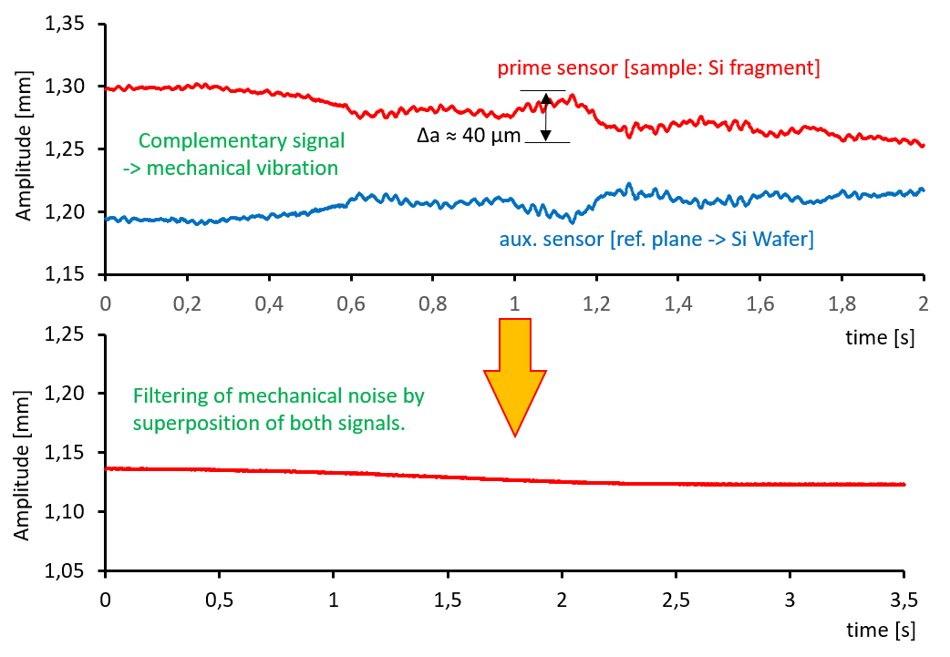
By scanning a plane Si-chunk, only vibration occur on the sensor signals. This can be observed in the top image, where both sensors show the same but complementary signal. By adding both signals, as shown in the bottom graph, the noise can be filtered out up to < 1µm.
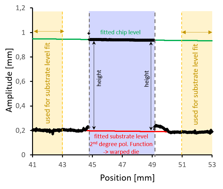
The image above shows a typical line scan and the procedure to calculate the heights out of it. The roughness of the substrate (ΔA ≈ 10 µm) is the limiting factor for accuracy. However, the roughness is repeatable, which lead to a stable repeatability of 1-2 µm for heights.
Out of 2-4 line scans, the BLT, the Tilt and the chip warpage can be calculated easily.
Demonstration video
info About
Innovation: 100% in-line inspection
proposes a new strategy as well as a new solution for integrating new measurement methods based on transient thermography into the production line for volume manufacturing of micro/nano-electronic components. This approach features novel and world’s first integrable thermographic failure analytical systems for 100% in-line inspection, which is in the focus of the project featuring also other key innovations enabling important aspects for future smart production:
- Exploitation of IR and TR as applied failure analytical method for in-line inspection by exploiting the introspective and physically most justified information of the thermal contrast obtained after pulsed energetic excitation of the component. The method produces already fair single-frame contrast, but reaches full potential by lock-in amplification. Both methods are full-field techniques and are more suitable than scanning techniques to enable fast 100% inspection. For that purpose, the systems feature automated sample feed, positioning, excitation and measurement capabilities.
- Extension of transient thermography to non-contact and reflective surfaces, which are not effectively measurable with infrared techniques but by the complementary method of thermoreflectance. This is highly desirable, as most chips are reflective at the surface in the optical spectrum (metals, semiconductors) where not polymer-passivated. So, both techniques allow monitoring of successive steps in the production process.
- Co-integration of periodic, customizable energetic excitation by various heat sources (radiative, inductive, convective) coupled to lock-in processing and a software environment for data preprocessing, evaluation and decision making respectively.
- High spatial resolution: The methods have the advantage of either mid-IR- or optical resolution (4 μm and 400 nm respectively). This is an advantage over time honored failure analytical techniques, even offline.
Demonstration and benchmarking at the production line under industrial boundary conditions
The in-line inspection systems based on PIRT and TR will be demonstrated at the SMEs and industrial component manufacturer’s at the line in a real industrial environment on a production run featuring a large number of micro/nano-electronic components, exemplified on power multi-chip modules from the industrial sectors of RF systems (GaN) and automotive (Si).
Benchmarks
To demonstrate the developed systems and demonstrators, several examples have been defined and tested using the project demonstrator to detect hidden flaws.
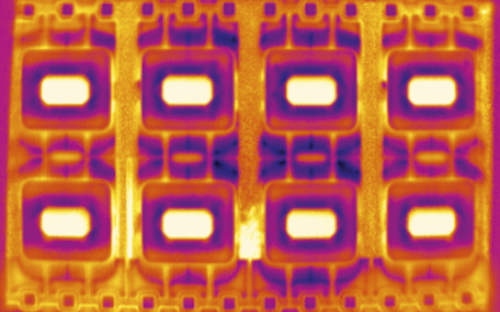
Molding compound
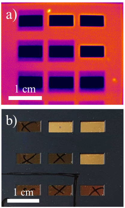
This example shows LGA chips in molding compound. The bright, yellow spots are void with few tens of micron in diameter.
Flaws in molding compound may influence the functionality and reliability of devices. As hidden flaws their detectability by optical methods as well as functional tests is greatly limited. Thermographic methods as developed in INLINETEST, in contrary, allow detection, localization and quantification of flaws such as voids or inclusions.
Carbon fiber reinforced polymer (CFRP)
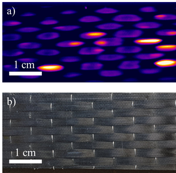
The given example is a carbon fiber reinforced polymer that has not been evacuated well enough, leaving remaining air in between the carbon fibers.
Leftover air or other included material in (carbon) fiber reinforced polymers can put the reliability of devices and components at high risk. The mechanical properties of substrates and other parts may change in unforseeable manner so that i.e. the CTE missmatch-driven warpage creates more stress than designed and would be uncritcal.
Sinter interconnect
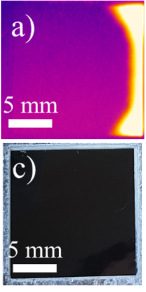
High quality sinter interconnects, ranging from die attach to large-area interconnects of substrates on baseplates, are key to performant, reliable and efficient components and systems. Cracks or delamination, however, are mostly impossible to find before a functional test is conducted, and even then the results may not obviously imply a flawed interconnect.
Typical methods, such as X-ray analysis are very expensive, time-consuming, not necessarily non-destructive and not even a safe bet to detect and localize a bad interconnect.
Analysis by thermographic methods are the ideal solution to qualify solder and sinter interconnects and are - thanks to INLINETEST - available as in-line quality assessment tool available in the near future.
Thermoreflectance test chip
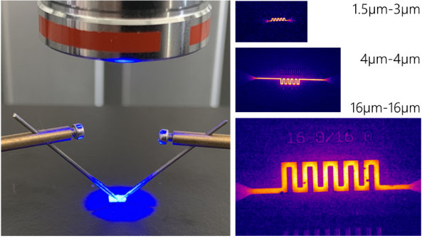
To evaluate the feasibility of thermoreflectance as method for failure analysis and quality assessment a dedicated test chip has been desgned and built that allows to test out different orders of magnitute in terms of spatial scale, time resolution and amplitude resolution.
The test chip includes test structures in single digit micron range and was used to prove a spatial resolution of 1 µm for the used thermoreflectance system. This is five times small than the physical limit of infrared thermography and underlines the potential of this technique.
Background
Micro- and nanoelectronic components are one key driver of today’s industrial growth and have been pervading nearly every domain of modern society and life, tendency: increasing. For that reason, it is a multi-billion-dollar business, extending from low profit margin but high volume consumer components to e.g. high value power and RF components. For the latter, component annual growth rates are predicted to exceed 20% (Source: Yole Development) for telecom, avionics and automotive applications, all of which are key segments of the European electronic industry.
In order to be competitive on these markets, components need to have high quality, i.e. be reproducible, robust and reliable under given environmental conditions. These quality issues are to a great deal determined by their production processes: This is where tolerances, flaws and defects are induced which are responsible for early malfunction of failure in field operation. It is reported that the costs for non-quality (e.g. repair, warranty, rejects) can amount to 5-8% of the turnover. The hidden costs (bad press, long time to market, dissatisfied customers, sinking sales figures), however, are estimated to go beyond 20% (Source: Gottschalk, Quality assurance of electronic components).
read moreQuality assurance is therefore of paramount importance and is an integral part of industrially implemented Total Quality Management, Zero Defect or Six Sigma strategies, which demand constant quality improvement. The key to highest productivity at highest yield and lowest cost is 100% in-line inspection during production, to gain intimate knowledge about interdependencies between process steps and process parameters. This paves the way to what is called smart production, where ample measured information concerning key parameters at each process step during production is available in real time to allow 100% individual traceability and immediate feedback in the framework of a big data correlation scheme.
True novelty in failure detection
INLINETEST targets the design, realization, deployment and test of two novel in-line inspection systems for micro/nano-electronic components. Thereby, the fast, contactless and non-destructive full-field thermometric methods of Pulse-Infrared Thermography (PIRT) and Thermoreflectance (TR) are exploited for the first time to enable 100% in-line production monitoring. This will be done by adapting and upgrading existing lab prototypes for both methods to the challenges of real-life in-line testing, enhanced by hard- and software innovations. For validation under real-life conditions, both failure analytical method’s hard- and software will be customized and integrated into two production lines and demonstrated on two encapsulated power multi-chip module (MCM) components and one in-line production tool at the project partners. Three global players in micro/nano-electronics in Europe accompany this endeavor on the board of industrial advisors.
Micro/nano-electronic components fail under field and test conditions due to thermal and mechanical overload or over time (fatigue failures), both of which are governed by the structural integrity of the component. This structural integrity, however, is determined during production by e.g. tolerances in material or processing parameters. This can lead to weak points in the component as e.g. voids, material gradients or inhomogeneity, cracks, delamination, dewetting, or geometric tolerances, impairing robustness and reliability:
- High power transients can damage the semiconductor by overheating due to local thermal hot spots or decisively reduce its lifetime due to the set-in of unwanted diffusion processes.
- Weak spots can lead to thermo-mechanical reliability issues like cracking or delamination.
For that reason, the consortium has decided to demonstrate the envisaged in-line inspection system on two power components from relevant European market segments with also silver sintered die attach material in application, designed also for use in harsh environment:
- A GaN RF HEMT HPA power MCM encapsulated component for avionics and telecom applications, using eutectic solder as die attach material and epoxy molding compound (EMC) encapsulant.
- A Si-based power MCM for automotive applications, using sintered silver as die attach material and an EMC encapsulant.
From Lab-Scale to In-Line Process
It is, however, important to note that the employed failure analytical techniques can also be in-line-applied to non-power components as e.g. advanced packages during ramp-up of consumer products.
The principle of the failure analytical methods on which the in-line inspection systems are based are highlighted in Figure 2. After transient energetic excitation, propagating thermal waves probe the heat path in the component which is determined by the material properties, i.e. also the structural integrity. Aberrations or anomalies can thus be made visible by recording the thermal signature of the component as response to that excitation. This thermal signature (surface temperature over time) is recorded either by PIRT or TR. As one can see, the methods are complementary in the sense that PIRT is sensitive for non-reflective surfaces (e.g. encapsulated components) whereas the other, TR, is sensitive to reflective surfaces. So many stages in the production process can be monitored. One major advantage is that the equipment probes exactly those flaws which are responsible for a later failure by the same physical effect of high temperature. So the thermal contrast detected by the two methods is physically very motivated and justified and better suited than time-honoured methods which, if at all in-line capable, monitor derived qualities as acoustic reflection or absorption of radiation. Further, cooling down time (tens of seconds) after processing can ideally be used for thermographic methods as it is not used otherwise.
So, new information on production process quality can be obtained which has so far been inaccessible, allowing countermeasures and control to potential aberrations in the process flow. This new information renders the production smarter and will thus enable higher yield, narrower tolerances, better reliability, less maintenance cost and thus result in a higher productivity, less waste and higher profits. Limitations of today’s in-line testing
For manufacturing of micro and nanoelectronic components in-line-capable failure analytical techniques must feature capability (detect/measure the defect in question), precision (how good the defect can be detected and differentiated from others without fault) and efficiency (measurements per unit time) by preferably non-contact methods.
The absence of insight: why INLINETEST is necessary
Whereas fast automated in-line equipment is available on the market, the bottlenecks are the respective measurement systems and the real-time data processing. Many methods are too slow to keep track of the production. Thermography is used today already for in-line measurements as it is a fast optical method, but only for approximate thermal resistance determination (e.g. LED). Electrical hot probing is an alternative, but not all samples allow to be electrically contacted at relevant production stages due to their complexity or sensitivity. So, whereas this is done and possible for LEDs on different complexity levels, it is much more complex for RF-circuits, and electrical response signals do not reveal a spatially resolved map of structural deviations from the standard. But a temperature contrast detected on reflective surfaces could. X-raying of samples, often a method of choice, is not sensitive to most surface or small scale defects, especially for low-Z elements (e.g. encapsulants, etc.)
The result is, that often indirect methods are applied, i.e. offline analysis by random sampling tests for process control followed by statistical schemes like six sigma to minimize the risk of failures in the field. Therefore, specifications of the components are chosen that typically reduce the production yield significantly which is of course not desirable.
Testing costs is another limitation which translates into test time and equipment cost. However, for newly designed, advanced high quality products, as targeted here, testing in production is required, and to widen the scope incorporating also thermo-mechanical parameters is highly desirable. The absence of defects is a figure of merit for the operation conditions that can be applied to the device. Thus, the determination of the structural integrity with a significant accuracy enables a unique selling point: performance will be improved according to the true capabilities of the device to sustain the applied thermal and mechanical load. In sum, today’s hard- and software solutions for in-line testing cannot reach out to the opportunities represented by thermography as established method for industrial application (high TRL) to the point that smart production can be leveraged up to a new level.
The consortium
The consortium consists of five companies from three different European countries: Germany, France and Netherlands. Assembled from members along the full value chain from fundamental method development via equipment supplying finally to in-line productions facilites ready to implement new standards in quality assessment.
Berliner Nanotest und Design GmbH
Nanotest, a small enterprise based in Berlin, is a well-established test equipment manufacturer for thermal characterization and failure analysis. They cover characterization of a wide range of materials from electronics industry and also offer thermal analysis of components and systems and sell their measurement systems to customers in various industries. Based on their experience in system development, thermal characterization and reliability assessment they builds the in-line inspection system of project .
visit homepageThales SA
Thales is a leading European microelectronic components and systems manufacturer and global player and is to test the in-line inspection system on their research production line for RF HEMT components.
visit homepageTechnische Universität Chemnitz
The academic side of project is represented by the Technische Universität Chemnitz, who has longstanding expertise in thermal and reliability engineering for test systems in cooperation with industry.
visit homepageAdvanced Packaging Center BV
The Advanced Packaging Center is a packaging specialist that develops, proto-types and produces special packaging solutions for the worldwide sensor and power semiconductor market. Advanced packaging Center owns a production line for micro/nano-electronic components and will test the novel equipment under real life conditions.
visit homepageBoschman Technologies BV
The SME Boschman Technologies is a specialist in developing and delivering Film Assist Molding equipment and Ag-sintering equipment for the worldwide semiconductor sensor and power market. Boschman Technologies comes in as an equipment/tool manufacturer to incorporate the envisaged equipment.
visit homepageDissemination

INLINETEST Website Launched
If you can read this you might probably have stumbled across the first major dissemination activity already. Our Website. This site will be one of our dissemination platforms and be used to provide you with public deliverables, papers and other, additional information. Stay tuned, stay in-line.
29-March-18
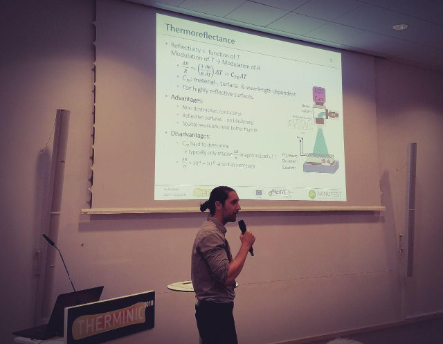
INLINETEST on Therminic 2018
Project partner Nanotest has presented their failure analysis ideas, concepts and recent progresses on the largest European conference on thermal phenomena in electronics: Therminic 2018. The conference took place in Stockholm and was hosted by Huawei and SHT. Dan Wargulski, a Nanotest employee, involved in the project, gave compehensive insights in latest achievements in both infrared-based and thermoreflectance-based thermography and discussed the pro's and con's of both methods with regard to failure analysis. The audience mainly consisting of thermal experts gave highly positive feedback and are surely eager to hear about the progress on next year's Therminic conference.
28-September-18
First INLINETEST newsletter released
The annual newsletter has been released, informing the public audience about the current state of progress and about the general project outline, such as our visionary goals, our scientific strategy and our plans and activities so far and in future. The newsletter is available here for download and also being published in social networks and distributed to business partners of the project consortium members.
22-December-18

Publications in 2018
-
D.R. Wargulski, F. Löffler et al.
Comparative die-attach failure analysis by thermoreflectance, lock-in infrared thermography and scanning acoustic microscopy
→ THERMINIC 2018, Stockholm, Sweden, 2018 -
F. Löffler, D. Wargulski et al.
Vergleichende Die-Attach-Fehleranalysen mittels Thermoreflectance, Infrarot-Thermografie und Ultraschallmikroskopie
→ IMAPS Herbstkonferenz 2018, Munich, Germany, 2018
22-December-18
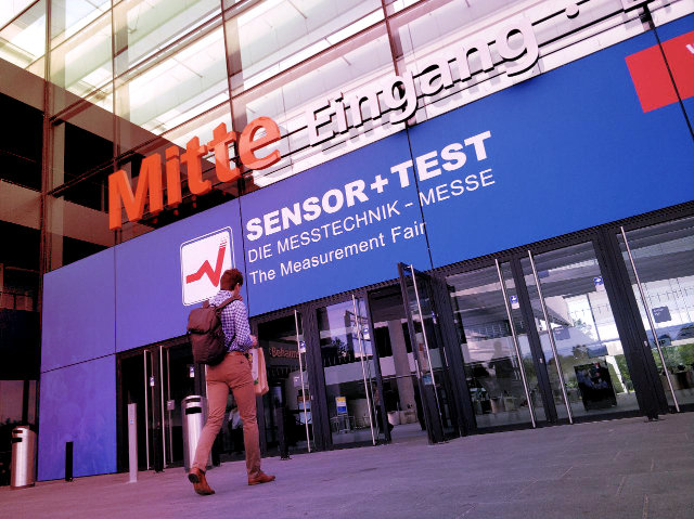
First public demonstration of INLINETEST results
The annual specialized fair SENSOR+TEST took place in Nuremberg in June 2019. This year, consortium member Nanotest hosted a booth demonstrating the first in-line quality assessment demonstrator based on project results. The demonstrator called INFAS (In-Line Failure Analysis System) raised many visitors' interest and was centerpiece of interesting discussion and exchange. The main finding was great interest in the topics of quality assessment and infrared thermography for failure detection. The combination of both seems even more promising to find a wide audience of potential customers.
17-July-19
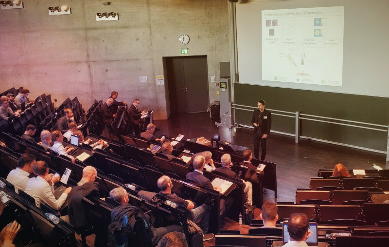
Presentation of INLINETEST on IMAPS Autumn Conference 2019
The IMAPS Autumn conference is a perfect venue to discuss the latest achievements in project INLINETEST. Dan Warguslki primarily talked about the chances and limits of IR-based failure analysis and initiated a vivid following discussion.
18-October-19
Publications in 2019
-
M. Abo Ras
New measurement and characterization equipment for thermal and thermo-mechanical effects
→ Chemnitzer Seminar “Zuverlässigkeit und funktionale Sicherheit”, Chemnitz, Germany, 2019 -
T. von Essen et al.
Innovative Techniques for Thermal Characterization and Inline-Capable Thermography-Based Failure Analysis
→ SENSOR+TEST 2019, Nuremberg, Germany, 2019 -
D. R. Wargulski, D. May et al.
An In-line Failure Analysis System based on IR Thermography ready for Production Line
→ THERMINIC 2019, Lecco, Italy
31-December-19
Second INLINETEST newsletter released
The annual newsletter has been released in a new issue. This time, we've got a lot of scientific and technical advancements we would like to bring to you. We've made big progress on many topics and already set up a functioning production line simulator for a QA system. Additionally, this newsletter give some information about how we spread the word and contribute to scientific knowledge exchange.
31-December-19
Publications in 2020
-
D. R. Wargulski, D. May, C. Grosse-Kockert et al.
Inspection of silver-sinter die attaches by pulsed and lock-in infrared thermography with flash lamp and laser excitation
→ QIRT 2020, e-conference -
D. R. Wargulski, D. May et al.
Inline failure analysis of electronic components by infrared thermography without high-emissivity spray coatings
→ ESTC 2020, e-conference -
D. R. Wargulski, D. May, J. Petrick et al.
Pulsed Infrared Thermography Failure Analysis of low-emissivity Specimens without contaminations caused by high-emissivity coatings
→ THERMINIC 2020, e-conference -
D. May, M. Gora, D. Wargulski et al.
Thermal Characterisation and Failure Analysis of MMIC Components by Thermo-Reflectance Imaging
→ THERMINIC 2020, e-conference -
T. von Essen, D. R. Wargulski et al.
IR based Failure Analysis of low-emissivity Specimens without sureface coatings
→ EuWoRel 2020, e-conference
23-December-20
newsletter the third
This third issue of the annual newsletter is the final regular one. As the project is going into overtime, more news will be published eventually, but not yet planned with a fixed date. So - stay tuned!
23-December-20
Contact us
Have questions regarding the project or the current state of the exploited results? Feel free to reach out to leader Nanotest: